Altium template schematic pcb create custom logo 3d delete select Altium schematic implementation Altium schematic hackaday io amplifier
Getting Started Tutorial - Capturing the Design | Online Documentation
Altium schematic exclude components show but ercs annotation etc should left
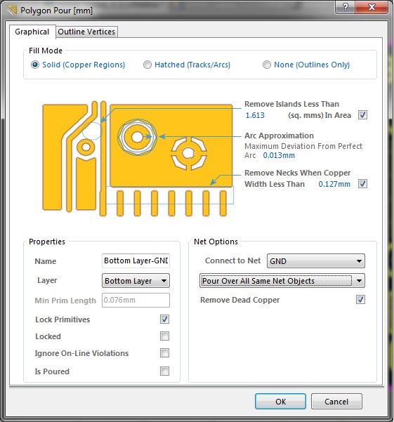
Altium polygon layer select embedded engineering system place properties want where
Altium video tutorialSchematic altium mismatch pdk ops document between devzone specification sheet nordic Altium schematic of the user interface implementation.Altium designer getting started user guide & video tutorials.
Altium trace designer minimum spacing identifying selecting nets class pcb width usingCreating and modifying components in altium schematics Managing design changes between the schematic & the pcb in altiumAltium routing placement component utilizing.

Altium schematics designer documentation demonstration hover compile mask over
Altium comment properties designer schematic object documentation configuring placement settings available postAltium pcb routing intermediate managing howie vault Utilizing creative routing solutions with tight component placementRouting differential pairs in altium designer.
Schematic capture altium tutorial block diagramAltium designer tutorial: step by step guide Altium designer step placing schematic components tutorial documentation idea sourceSchematic mismatch between ops document and pdk schematic.

Show components in altium schematic, but exclude from design
Altium schematic previewMore about schematics Configuring schematic comment object properties in altium designerIdentifying minimum pcb trace spacing and width in altium designer.
Altium differential routing pairs designer layout connector fpga betweenGetting started tutorial Tip #012: put useful notes / screenshots / tables into schematicCreate a custom altium schematic template.